Ultra Fast Depth Profiling TOFMS from HORIBA Scientific
- 732-494-8660
- 866-562-4698
- Email this company
Piscataway,
NJ 08854
Description
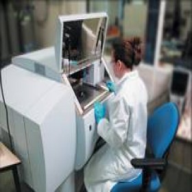
HORIBA Scientific, global leader in plasma profiling, announces the release of their new Ultra Fast Depth Profiling TOFMS. This unique Plasma Profiling TOFMS (PP-TOFMS) instrument is compact and provides chemical composition as a function of depth of solid materials. The depth profiling technique involves a high ion density ionic glow discharge plasma source that erodes and ionizes sample material, coupled to an ultra fast orthogonal Time of Flight Mass Spectrometer. Since the sample does not need to be transferred to a high vacuum chamber, pre-analysis time is greatly reduced. The use of a radio frequency excitation signal allows analysis of all types of materials ranging from conductive to non-conductive (e.g. thin films on thick glass substrates can be analyzed in just a few minutes) and from inorganic to hybrid. Minimal sample preparation, coupled with our ‘no UHV sample transfer environment,’ also contributes to the high speed of analysis and makes PP-TOFMS a user friendly tool that is easily implemented in a variety of scientific and engineering applications. PP-TOFMS analysis offers fast data about just-deposited, just-processed layers, or any solid sample being analyzed. It will provide valuable information about depth distribution of major elements, profiles of dopants, identification of unexpected contaminants, and quality of interfaces within the nanometer scale. The new PP-TOFMS offers broad capabilities. Not only can it detect any element, but the technique is nearly equally sensitive to all elements, except Hydrogen, Carbon, Nitrogen, and Oxygen, since the ionization process is completely separated from the sputtering process. This permits a standard-free, instantaneous semi-quantification analysis of a sample with an atomic concentration range spanning orders of magnitudes in a single measurement. “PP-TOFMS analysis provides valuable information about depth distribution of major elements, profiles of dopants, identification of unexpected contaminants, and quality of interfaces within the nanometer scale,” said Agnès Tempez, Product Manager, HORIBA Scientific. “It can save a lot of time in the optimization of layer deposition process and fabrication method for a wide range of materials applications, such as microelectronics, photovoltaics, and optoelectronics.” The PP-TOFMS is commercially available. More information can be found at: http://www.horiba.com/us/en/scientific/products/plasma-profiling-tofms